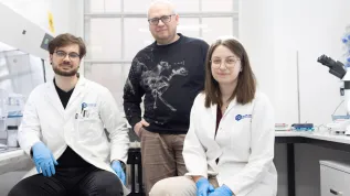
Flexible screens for TVs and smartphones that can be rolled up like a canvas painting, are the technologies on which global manufacturers of these devices are working. Laboratory in Łódź is testing organic materials which are used in such displays. "It is a transition from traditional LED technology to OLED technology" - told PAP Dr. Małgorzata Maciejczyk.
One of the latest laboratories in Technopark Łódź is the Laboratory of Biosensors and Bioelectronics, which tests the organic materials used in displays of devices including TVs, laptops and smartphones.
The lab also conducts research into optimisation of conditions for manufacturing devices from organic materials and their composites. It can design and characterize the properties of organic light emitting diodes (OLED) used in graphic displays, photovoltaic cells and field-effect transistors.
Dr. Małgorzata Maciejczyk told PAP that the laboratory currently focuses on the broader printed electronics. "It is a transition from traditional LED technology to OLED technology, organic light emitting diodes that are used in flexible screens that can be rolled up, or smartphones, which can be bent and do not break" - she explained.
The Laboratory of Biosensors and Bioelectronics has a system of glove boxes with the latest solutions and research equipment. It allows to test the materials typically used in bioelectronics under inert gas conditions, oxygen and moisture-free. This ensures the highest quality of manufactured products.
As a result, specialists can verify whether the idea for the application of customer-supplied material is appropriate for bioelectronics technology, and whether it can be marketed.
The laboratory has also specialized inkjet printer, which allows you to print optoelectronic devices (transistors) or their components.
"We print entire devices or components that are used in optoelectronics, active layers of luminescent materials and conductive tracks from materials containing, for example, nanosilver. The printer can deliver a base of the device, or the entire, operational unit, namely light emitting diodes or transistors" - explained the laboratory manager Dr. Sylwia Kotarba.
The laboratory also has a unique, designed specifically for the Laboratory of Biosensors and Bioelectronics, fully automated measuring system, including a nanobot. It allows to study the electrical properties of OFETs (organic field effect transistor), which are lightweight devices, and the technology of their manufacture is simple and energy efficient.
In the future, based on these devices the laboratory in Łódź wants to design and produce easy to miniaturize type of sensors that can be used in personalized medicine.
"This set of devices allows to manufacture not only transistors or OLEDs, but also sensors based on them. This can be used in personalized medicine, for example in testing blood glucose that could be coupled with a mobile device so that the carer can remotely monitor the patient\'s condition" - explained Dr Kotarba.
The Laboratory of Biosensors and Bioelectronics is part of the BioNanoPark - one of the most advanced research and implementation centres for business, which is a part of the Łódź Regional Park of Science and Technology. The largest shareholders of Technopark are the city of Łódź and the Łódź province, other shareholders include Lodz University of Technology.
For three years now, biotechnology and nanotechnology labs conduct research for the chemical, cosmetic, pharmaceutical, food and fuel industries.
Since the beginning of this year, Technopark has six new laboratories with modern equipment, including the unique, designed and built by Polish specialists ARUZ, called a "digital test tube" which has more computing power than supercomputers. There are also laboratories specialising in biotechnology, personalized medicine, product authentication and molecular simulations. (PAP)
szu/ ksk/
tr. RL


