Scientists from the Warsaw University of Technology have developed a computational imaging method that can precisely measure semiconductor nanostructures from a single optical image, potentially speeding up quality control in photonic chip manufacturing and quantum technologies.
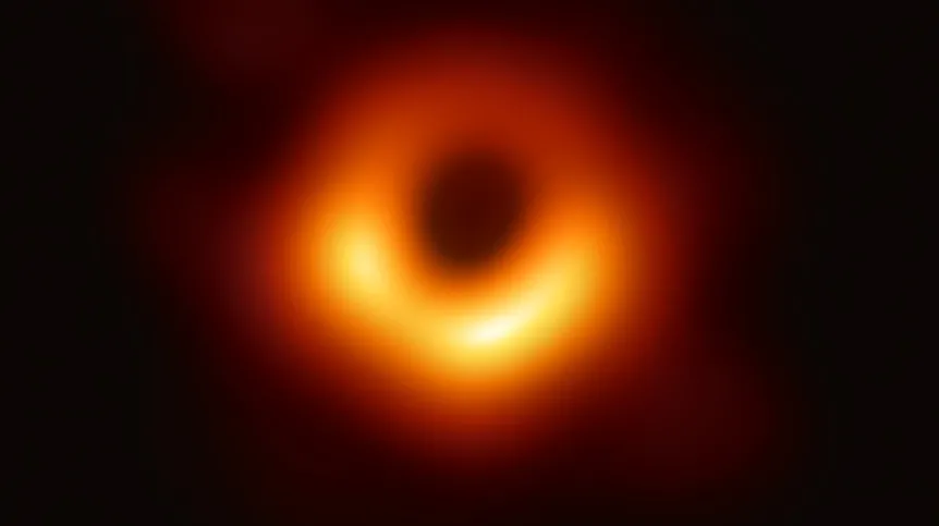
The research, led by Maciej Trusiak, applies Bayesian inference techniques similar to those used in producing the first image of a black hole to the imaging of nanoscale semiconductor components. The findings were published in the journal Laser & Photonics Reviews.
Trusiak, a recipient of a European Research Council grant, developed the method with contributions from Damian Suski and Maria Cywińska. The technology is designed to determine the geometry of nano-objects too small to be resolved directly by conventional optical systems.
“If scientists knows what they are looking for, an algorithm can help spot it even where it is seemingly invisible. This was the case with the first black hole images, and it can be the same in computational imaging of nanoscale objects”, Trusiak told PAP - Science in Poland.
The researchers focused on semiconductor waveguides used in photonic integrated circuits, or PICs, which are considered key components in next-generation computing systems.
“Semiconductor structures are the foundation of today's computing chips. AI models run on them. Companies like those in Taiwan are successful because they can design and manufacture such components with exceptional precision. However, this requires the ability to measure structures that are invisible to the naked eye. Our work concerns such measurements, specifically waveguides - channels through which photons travel in the latest generation of photonic processors (PICs)”, Trusiak said.
The structures studied are only a few to several nanometres high — roughly 10,000 times thinner than a human hair and less than 100 atoms across. Existing measurement techniques such as atomic force microscopy are highly precise but slow and potentially damaging to delicate materials.
“We were looking for a way to do this over a large field of view, non-invasively, and with light”, Trusiak said.
The new approach uses interferometry, in which a beam of light is split into an object beam and a reference beam. When recombined, the beams create interference fringes encoding the three-dimensional structure of the object. Traditional interferometric methods typically require multiple images and precise mechanical adjustments.
The Warsaw team’s method instead relies on analysing a single interferometric image using a Bayesian algorithm known as Dynamic Nested Sampling.
According to the researchers, the system can detect structures hidden in noise that conventional image analysis methods would miss. The algorithm generates statistical models of the object and calculates how closely they match the recorded image, allowing scientists to estimate nanostructure geometry and measurement uncertainty simultaneously.
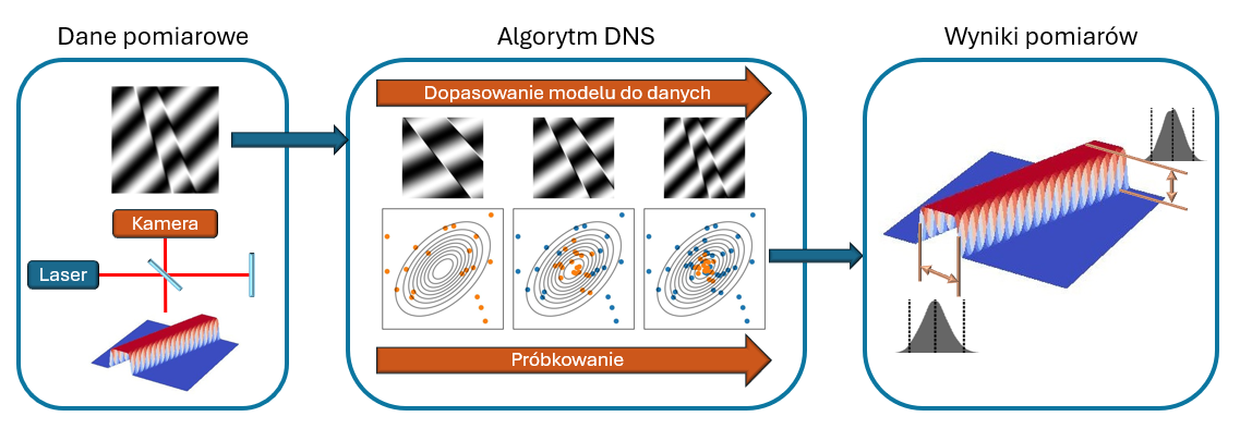
The method was experimentally validated in collaboration with researchers from the University of Tromsø on structures measuring 8 and 15 nanometres in height. The results closely matched reference measurements obtained using atomic force microscopy.
Trusiak said the technology could help manufacturers rapidly verify whether semiconductor structures produced through photolithography match their intended designs.
“Manufacturers of machines for the production of nanostructures by photolithography have ready-made 3D models of the structures they want to create. Our algorithm can verify whether what comes off the production line matches the design without having to scan each chip for hours”, he said.
The researcher said the project demonstrates how techniques developed in one scientific field can be adapted to another.
“Modern LED lighting was not created by improving the candle. My example shows that sometimes it is worth risking using a technique from a completely different scale and recognising that data is just data - regardless of whether it comes from a telescope or a microscope - and using everything we know about the object under study instead of measuring blindly”, Trusiak concluded.
PAP - Science in Poland, Ludwika Tomala
tr. RL
lt/ zan/